Research Areas
Micro Transfer Printing
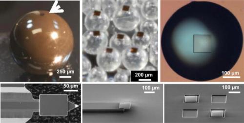
As a process, micro-transfer printing provides a unique and critical manufacturing route to extracting active microstructures from growth substrates and deterministically assembling them into a variety of functional substrates ranging from polymers to glasses and ceramics and to metallic foils to support applications such as flexible, large-area electronics, concentrating photovoltaics and displays. Laser transfer printing extends micro-transfer printing technology by providing a non-contact approach that is insensitive to the preparation and properties of the receiving substrate. It does so by exploiting the difference in the thermo-mechanical responses of the microstructure and transfer printing stamp materials to drive the release of the microstructure or ‘ink’ from the stamp and its transfer to substrate.
Key Publications:
- Reza Saeidpourazar et al, “A prototype printer for laser driven micro-transfer printing”, 2012, Journal of Manufacturing Processes, Vol 14, Issue 4, pp. 416.
- Ala’a M. Al-okaily et al, “Characterization of Delamination in Laser Microtransfer Printing”, 2014, J. Micro Nano-Manuf., Vol. 2(1), pp. 011002.
Solid State Superionic Stamping (S4)
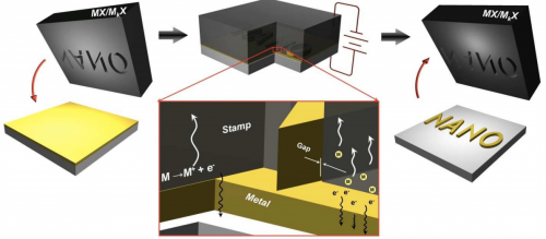
S4 is a solid-state electrochemical nanoimprint process for direct patterning of metallic nanostructures. It uses a patterned solid electrolyte or superionic conductor (such as silver sulfide) as a stamp and etches a metallic film by an electrochemical reaction. Our preliminary experiments demonstrate repeatable and high-fidelity pattern transfer with features down to 50 nm on silver films of thicknesses ranging from 50 to 500 nm. As the process is conducted in an ambient environment and does not involve the use of liquids, it displays potential for single-step, high-throughput, large-area manufacturing of metallic nanostructures. The use of superionic conductors in manufacturing opens up a new and potentially energy-efficient approach to nanopatterning and fabrication. It offers a highly competitive approach, both as a stand-alone process and as a complement of other nanofabrication techniques, to fabricating chemical sensors, photonic and plasmonic structures, and electronic interconnects.
Key Publications:
- Kyle Jacobs et al, “Solid-state superionic stamping with silver iodide–silver metaphosphate glass”, 2011 Nanotechnology, Vol. 22, pp. 425301.
- Bruno Azeredo et al, “Silicon nanowires with controlled sidewall profile and roughness fabricated by thin-film dewetting and metal-assisted chemical etching”, 2013, Nanotechnology, Vol. 24, pp. 225305.
- Bruno Azeredo et al, “Direct Imprinting of Porous Silicon via Metal‐Assisted Chemical Etching”, 2016, Advanced Functional Materials, Vol. 26, Issue 17, pp. 2929-2939.
- Shama Farabi, “Electrochemical direct writing and erasing of silver nanostructures on phosphate glass using atomic force microscopy”, 2017, Nanotechnology, Vol. 28, Issue 6, pp. 065301.
MEMS Positioning and Manipulation Systems
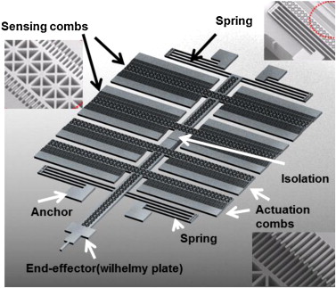
We developed a single degree-of-freedom probe that is capable of regulating an input position and measuring force or applying a constant input force and measuring deflection. Such a probe is useful in making sensitive measurements on thin films, nano- and microstructures, and fluids. The probe is actuated by an electrostatic comb drive with an integrated capacitive sensor. COTS electronics and a capacitance-to-voltage IC are used to develop a closed-loop controller for the system, capable of regulating position over a range of about 40 μm to within a 5 nm resolution and controlling forces up to 300 μN with a resolution of 25 nN.
Key Publications:
- Bonjin Koo et al., “An active MEMS probe for fine position and force measurements”, 2014, Precision Engineering, Vol. 39, pp. 738.
- Jorge Correa et al., “Laminated micro-machine: Design and fabrication of a flexure-based Delta robot”, 2016, Journal of Manufacturing Processes, Vol. 24, pp. 370-375.
- Jorge Correa et al, “Parallel-kinematics XYZ MEMS part 1: Kinematics and design for fabrication”, 2015, Precision Engineering.
- Bonjin Koo et al., “Parallel-kinematics XYZ MEMS Part 2: Fabrication and Experimental Characterization”, 2016, Precision Engineering.